CD4047 Pinout
The CD4047 is a low-power CMOS multivibrator IC commonly used in inverter circuits, oscillator applications, and timing circuits. It can operate in astable mode to generate continuous square-wave signals or in monostable mode to produce a single timed pulse.
In a basic push-pull inverter design, the CD4047 generates complementary output signals that can control a suitable MOSFET gate-driver stage. The switching stage then converts energy from a DC source into an alternating waveform through a transformer.
Image: Insert a CD4047 IC pinout diagram here.
Materials Required
The components used in a CD4047-based inverter depend on the required input voltage, output voltage, power rating, and transformer configuration.
- CD4047B CMOS multivibrator IC
- Suitable MOSFET gate-driver circuit
- Power MOSFETs selected according to the design requirements
- Appropriately rated transformer
- Timing resistor and capacitor
- IC supply-decoupling capacitors
- DC input source with suitable current capacity
- Input fuse and overcurrent protection
- MOSFET heat sinks and thermal management components
- Printed circuit board (PCB)
- Suitable electrical connectors and insulated enclosures
- Multimeter and appropriate electrical test equipment
Important: A CD4047 inverter is not automatically a 1,000-watt inverter. The MOSFETs, transformer, driver, PCB conductors, protection components, and cooling system must all be engineered for the intended power level.
How a CD4047 Inverter Works
The operation of a CD4047-based inverter can be divided into four main stages.
1. Oscillator stage
The CD4047 generates periodic timing signals. In astable mode, its complementary outputs can provide alternating control signals for a push-pull switching arrangement.
2. Gate-driver stage
A dedicated gate driver may be needed to provide the current required to switch the MOSFET gates quickly and reliably. The CD4047 itself is not designed to drive a high-power switching stage directly.
3. Power-switching stage
The MOSFETs switch current through the transformer primary in an alternating sequence. The switching frequency and transformer configuration must be compatible with the design.
4. Transformer output stage
The transformer transfers energy from the low-voltage DC switching circuit to a higher-voltage AC output. The resulting waveform may be a square wave or modified waveform rather than a pure sine wave.
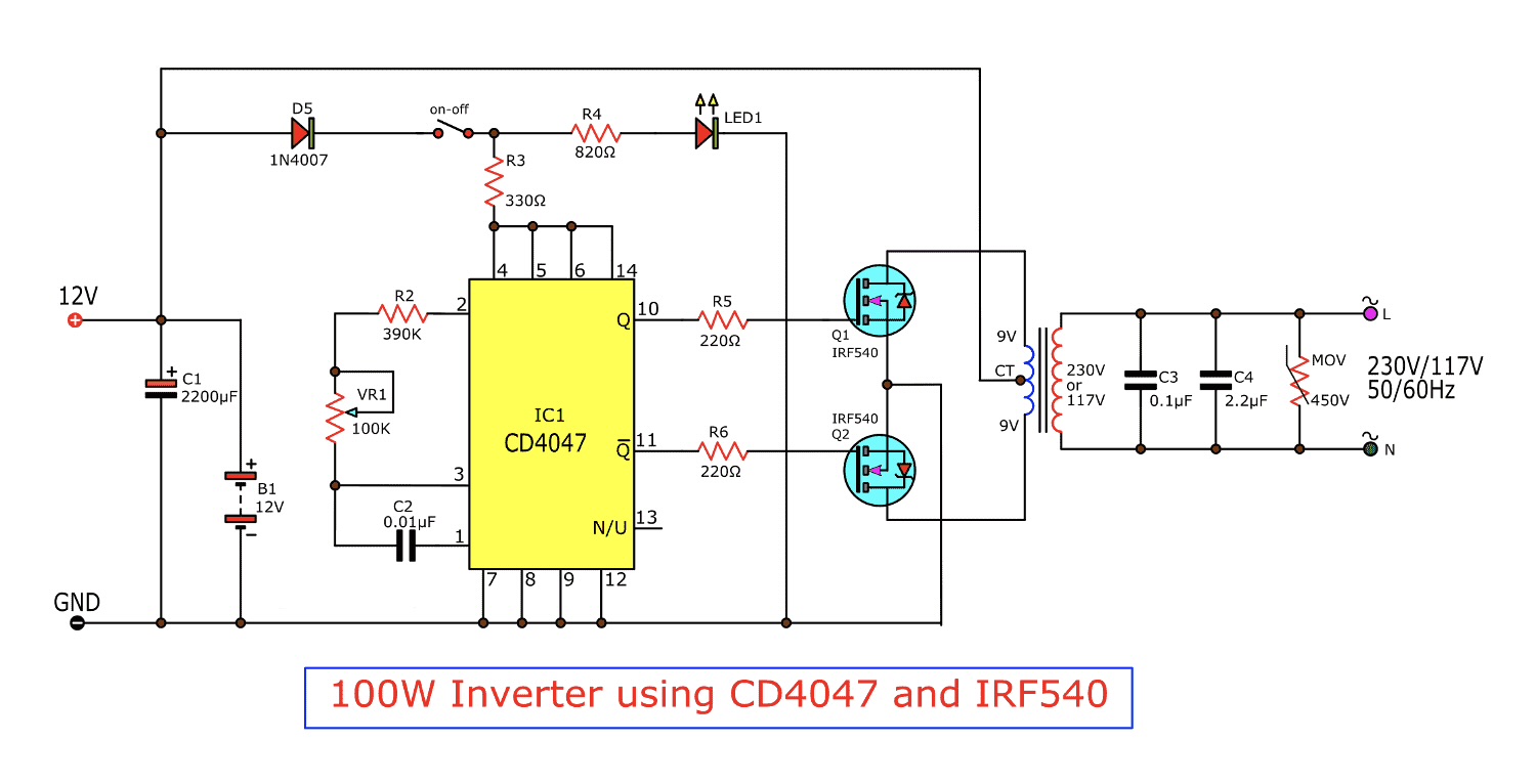
Circuit Diagram
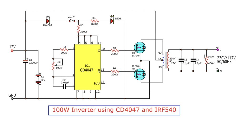
A complete schematic should identify the oscillator connections, gate driver, MOSFET switching stage, transformer winding configuration, DC input protection, and output protection. Component values and connections must be selected for the specific design rather than copied from an unrelated inverter circuit.
Important Design Considerations
1. Oscillator frequency
The CD4047’s timing resistor and capacitor determine its oscillation timing. The required frequency depends on the circuit configuration and transformer design. Verify the actual output frequency against the IC datasheet and the intended operating conditions.
2. MOSFET selection
MOSFET selection depends on the DC bus voltage, current, switching frequency, gate-drive voltage, conduction losses, and thermal limits. A suitable gate driver and adequate protection are essential for reliable operation.
3. Transformer rating
The transformer must be designed for the intended switching frequency, input voltage, output voltage, and load. An unsuitable transformer can overheat or saturate even when its advertised power rating appears adequate.
4. Cooling and protection
High-current inverter circuits can generate substantial heat. Proper thermal design, overcurrent protection, appropriate fusing, and a suitable enclosure are necessary.
5. Output waveform
A basic CD4047 push-pull inverter generally produces a square-wave-type output. Devices designed for sinusoidal AC may require a properly engineered pure-sine-wave inverter instead.
Applications of CD4047 Inverters
CD4047-based inverter designs are useful for studying oscillator circuits, transformer switching, and basic DC-to-AC conversion. Depending on the complete design, related inverter architectures may be used in backup-power systems, educational electronics projects, and selected low-power applications.
Safety Precautions
Inverter circuits can involve high battery currents and potentially lethal AC output voltages. A battery can also deliver enough current to cause severe burns, fires, or component failure.
- Never assume that a circuit is safe because its input voltage is only 12 V.
- Do not connect an experimental inverter directly to household wiring.
- Use appropriate fusing, insulation, enclosure design, and electrical protection.
- Have high-voltage testing and commissioning performed or supervised by a qualified electronics professional.
- Verify transformer connections and component ratings against a complete, validated schematic before energizing the circuit.
Conclusion
The CD4047 is a useful IC for generating complementary timing signals in push-pull inverter designs. Combined with an appropriately designed gate driver, power-switching stage, and transformer, it can form part of a DC-to-AC conversion system.
However, achieving a reliable inverter requires more than connecting a timer IC to MOSFETs and a transformer. Frequency selection, switching losses, transformer design, thermal management, and electrical protection all play important roles. For a practical inverter project, use a validated schematic designed for the intended voltage and power rating, and ensure that high-voltage testing is carried out safely.