Conversion of AC to AC is quite simple as in compare to DC to DC converter because it only implies a transformer which converts AC from one voltage level to another voltage level.
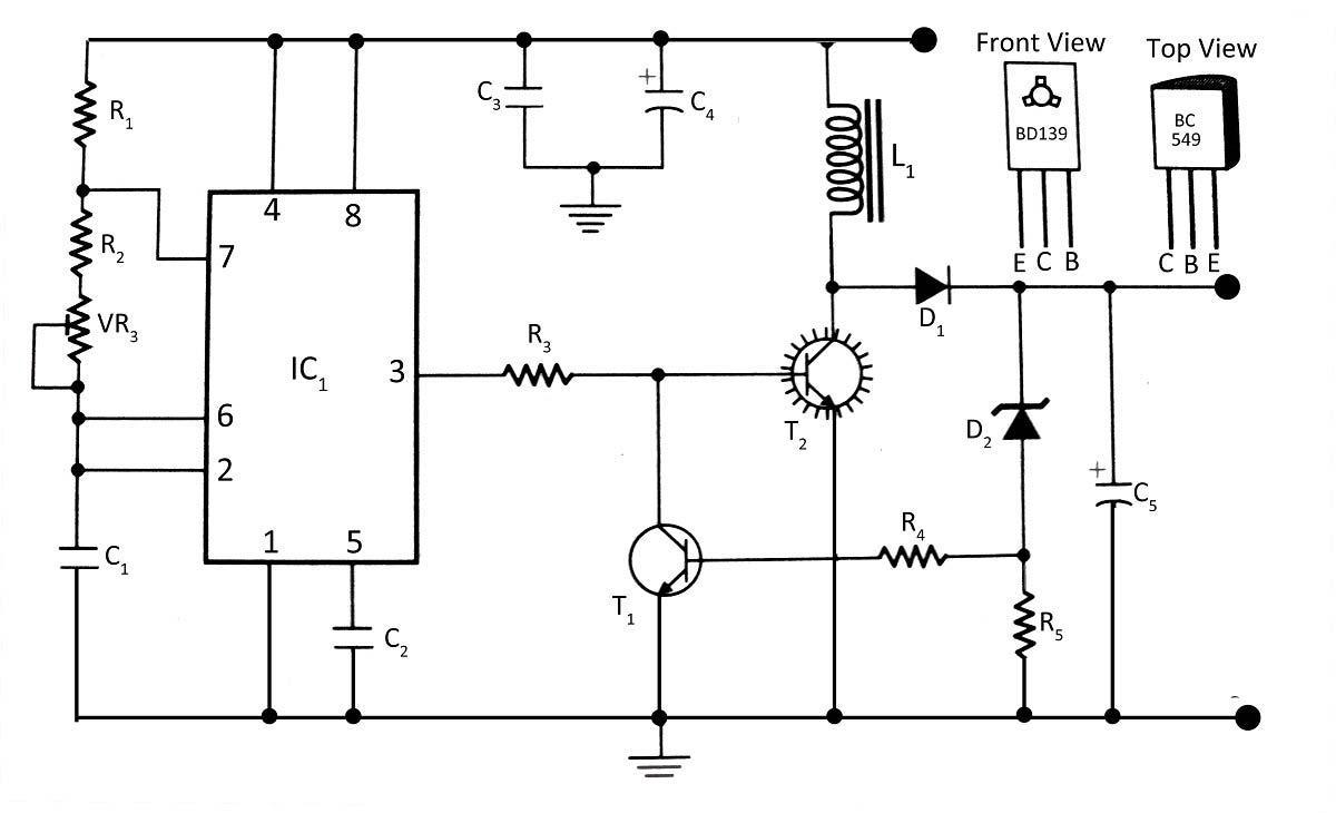
But conversion of DC to DC is quite tedious work without transformer and more power losses. The archived circuit below uses a 555 timer and an inductor to step up a DC supply. It is a boost converter, rather than a capacitor-only voltage doubler. Its intended application is approximately 6 V to 12 V, but output voltage, available current and efficiency have not been verified here. Treat it as a circuit to study, not a tested power supply.
The circuit of DC to DC conversion is build with a very popular IC LM555 used as multivibrator mood which generate required frequency range from 2 to 10 kHz to drive power transistor T2. Here potentiometer VR1 is used to adjust output frequency given to transistor T2 via resistor R3. A zener diode in this circuit is used as voltage regulator which regulates voltage to 12 volt.
Inductor parameters
Here Inductor L1 of 100 turns, 24 SWG enameled copper wire wounded on a 40mm dia. toroidial ferrite core and capacitor C5 is employed for energy storage. Transistor T1 is used to control output control with the help of resistor R4 R5.
The circuit diagram
Component part list
Resistors (all ¼-watt, ± 5% Carbon)
R1, R2, R5 = 10 KΩ; R3, R4 = 220 Ω 1/2-watt; VR1 = 47 KΩ Capacitors
C1 = 0.0047 µF; C¬2 = 0.01 µF; C3 = 0.1 µF; C4 = 470 µF/25V; C5 = 2200 µF/35V Semiconductors
D1 = 1N4007; D2 = 12 V zener diode, ½-watt (this power rating does not specify the converter output current); T1 = BC549; T2 = BD139; IC1 =
NE555 timer IC
Miscellaneous
L1 = 100 Turns, 24 SWG insulated copper wire on 40mm Dia. toroidal core
What to verify before using this circuit
The inductor stores energy while T2 conducts. When T2 switches off, current flows through D1 to the output capacitor and load. The zener and T1 form a feedback path that reduces drive as the output rises. A 12 V zener does not imply an exact 12.00 V output because transistor junction voltage and component tolerances also affect the feedback threshold.
The winding description above is incomplete for a repeatable design: core material, inductance and saturation current are not specified. Do not infer a safe output-current rating from the transistor or zener alone. Check the diode switching characteristics, transistor pinout, capacitor polarity and voltage ratings against the actual parts. Use a current-limited low-voltage bench supply and a suitable resistive test load; measure output voltage, ripple, input current and component temperature before connecting electronics. This circuit provides no isolation between input and output.
For the underlying topology, see Texas Instruments’ Switching Regulator Fundamentals. For a practical regulated supply, choose a converter with a documented input range, output-current rating and protection specifications.